For semiconductors, our patented system for ball grid array assembly molds offers universal capabilities for virtually all BGA and MAPs.
The Neu Dynamics system allows for changes in package size from cycle to cycle with minimal down time. Development of advanced packaging systems for Ball Grid Array (BGA,) Quad Flat No Lead (QFN,) wafer level, stacked die, Micro Electro Mechanical Systems (MEMS,) Multi Chip Modules (MCM,) optical and LED devices is also part of our ongoing leadership in this latest encapsulation technology.
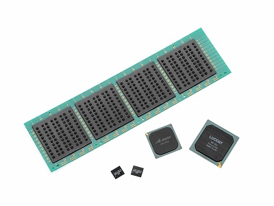
Our semiconductor packaging capabilities include:
- Discrete package
- Lead frame IC package
- RF module
- Diode components
- Tape base package
- Image sensor & optical device
- LED devices
- Power package
- Laminate package
- Chip scale package
- SIP module
- Ceramic and hermetic package
- Memory card
Contact us today to learn more about this process or to get started on your next project.